9
The OC trip point varies with MOSFETs temperature. To avoid
over-current tripping in the normal operating load range,
determine the R
OCSET
resistor from the equation above with:
1. The maximum r
DS(ON)
at the highest junction temperature.
2. The minimum I
OCSET
from the specification table.
3. Determine I
PEAK
for I
PEAK
> I
OUT(MAX)
+ (擨)/2,
where 擨 is the output inductor ripple current.
For an equation for the output inductor ripple current see the
section under component guidelines titled Output Inductor
Selection.
OUT1 Voltage Program
The output voltage of the PWM converter is programmed to
discrete levels between 1.3V
DC
and 3.5V
DC
. This output is
designed to supply the microprocessor core voltage. The
voltage identification (VID) pins program an internal voltage
reference (DACOUT) through a TTL-compatible 5-bit
digital-to-analog converter. The level of DACOUT also sets
the PGOOD and OVP thresholds. Table 1 specifies the
DACOUT voltage for the different combinations of
connections on the VID pins. The VID pins can be left open
for a logic 1 input, because they are internally pulled up to
+5V by a 10糀 (typically) current source. Changing the VID
inputs during operation is not recommended. The sudden
change in the resulting reference voltage could toggle the
PGOOD signal and exercise the over-voltage protection.
The 11111 VID pin combination resulting in an INHIBIT
disables the IC and the open-collector at the PGOOD pin.
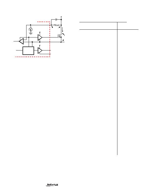
UGATE
OCSET
PHASE
OVER-
CURRENT1
+
-
GATE
CONTROL
VCC
OC1
200?/SPAN>A
V
DS
I
D
V
SET
R
OCSET
V
IN
= +5V
OVER-CURRENT TRIP: V
DS
> V
SET
(i
D
" r
DS
(ON) > I
OCSET
" R
OCSET
)
I
OCSET
+
+
FIGURE 9. OVER-CURRENT DETECTION
PWM
V
PHASE
= V
IN
- V
DS
V
OCSET
= V
IN
- V
SET
DRIVE
HIP6018B
VCC
LGATE
PGND
TABLE 1. V
OUT1
VOLTAGE PROGRAM
PIN NAME
NOMINAL
OUT1
VOLTAGE
DACOUT
VID4 VID3 VID2 VID1 VID0
0
1
1
1
1
1.30
0
1
1
1
0
1.35
0
1
1
0
1
1.40
0
1
1
0
0
1.45
0
1
0
1
1
1.50
0
1
0
1
0
1.55
0
1
0
0
1
1.60
0
1
0
0
0
1.65
0
0
1
1
1
1.70
0
0
1
1
0
1.75
0
0
1
0
1
1.80
0
0
1
0
0
1.85
0
0
0
1
1
1.90
0
0
0
1
0
1.95
0
0
0
0
1
2.00
0
0
0
0
0
2.05
1
1
1
1
1 INHIBIT
1
1
1
1
0
2.1
1
1
1
0
1
2.2
1
1
1
0
0
2.3
1
1
0
1
1
2.4
1
1
0
1
0
2.5
1
1
0
0
1
2.6
1
1
0
0
0
2.7
1
0
1
1
1
2.8
1
0
1
1
0
2.9
1
0
1
0
1
3.0
1
0
1
0
0
3.1
1
0
0
1
1
3.2
1
0
0
1
0
3.3
1
0
0
0
1
3.4
1
0
0
0
0
3.5
NOTE: 0 = connected to GND or V
SS
, 1 = open or connected to 5V
through pull-up resistors.
HIP6018B
发布紧急采购,3分钟左右您将得到回复。
相关PDF资料
HIP6021CB-T
IC REG QD BCK/LINEAR 28-SOIC
HIP6521CB-T
IC REG QD BCK/LINEAR SYNC 16SOIC
HMC920LP5E
IC CTRLR ACTIVE BIAS 32QFN
IDTTSE2002B3CNRG
IC TEMP SENS EEPROM DFN-8
IPM6220ACAZ-T
IC REG 5OUT BUCK/LDO SYNC 24SSOP
IR2170
IC CURRENT SENSE 600V 1MA 8-DIP
IR2171STR
IC CURRENT SENSE 8SOIC
IR2172S
IC CURRENT SENSE 8SOIC
相关代理商/技术参数
HIP6018CB
制造商:Rochester Electronics LLC 功能描述:- Bulk 制造商:Harris Corporation 功能描述:
HIP6018CB-T
制造商:Rochester Electronics LLC 功能描述:- Tape and Reel
HIP6018EVAL1
制造商:INTERSIL 制造商全称:Intersil Corporation 功能描述:Advanced PWM and Dual Linear Power Control
HIP6019
制造商:IRF 制造商全称:International Rectifier 功能描述:5-BIT PROGRAMMABLE SYNCHRONOUS BUCK, NON-SYNCHRONOUS,ADJUSTABLE LDO AND 200mA ON-BOARD LDO
HIP6019B
制造商:INTERSIL 制造商全称:Intersil Corporation 功能描述:Advanced Dual PWM and Dual Linear Power Control
HIP6019B_05
制造商:INTERSIL 制造商全称:Intersil Corporation 功能描述:Advanced Dual PWM and Dual Linear Power Control
HIP6019BBCB WAF
制造商:Harris Corporation 功能描述:
HIP6019BCB
功能描述:IC REG QD BCK/LINEAR 28-SOIC RoHS:否 类别:集成电路 (IC) >> PMIC - 稳压器 - 线性 + 切换式 系列:- 标准包装:2,500 系列:- 拓扑:降压(降压)同步(3),线性(LDO)(2) 功能:任何功能 输出数:5 频率 - 开关:300kHz 电压/电流 - 输出 1:控制器 电压/电流 - 输出 2:控制器 电压/电流 - 输出 3:控制器 带 LED 驱动器:无 带监控器:无 带序列发生器:是 电源电压:5.6 V ~ 24 V 工作温度:-40°C ~ 85°C 安装类型:* 封装/外壳:* 供应商设备封装:* 包装:*